Products
Nanotronics Inspection Systems — nSpec Automated Optical Inspection (AOI)
nSpec systems combine computer vision, AI, optical inspection equipment and robotics to support automated inspection workflows in R&D and high-volume manufacturing.
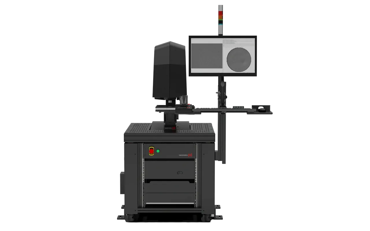
nSpec LS
Designed to streamline R&D efforts and optimize process improvements.
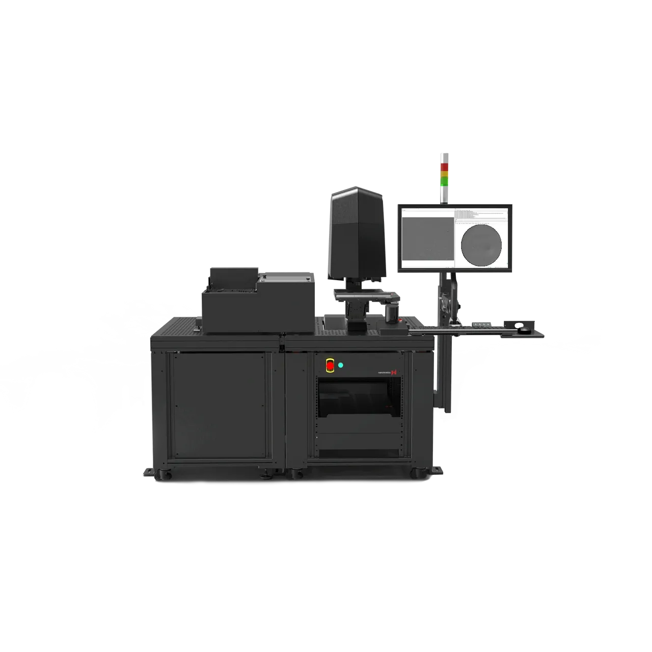
nSpec PS
Automate inspection from R&D to production with a single tool. Flexible software supports recipe configuration and evolution over time.
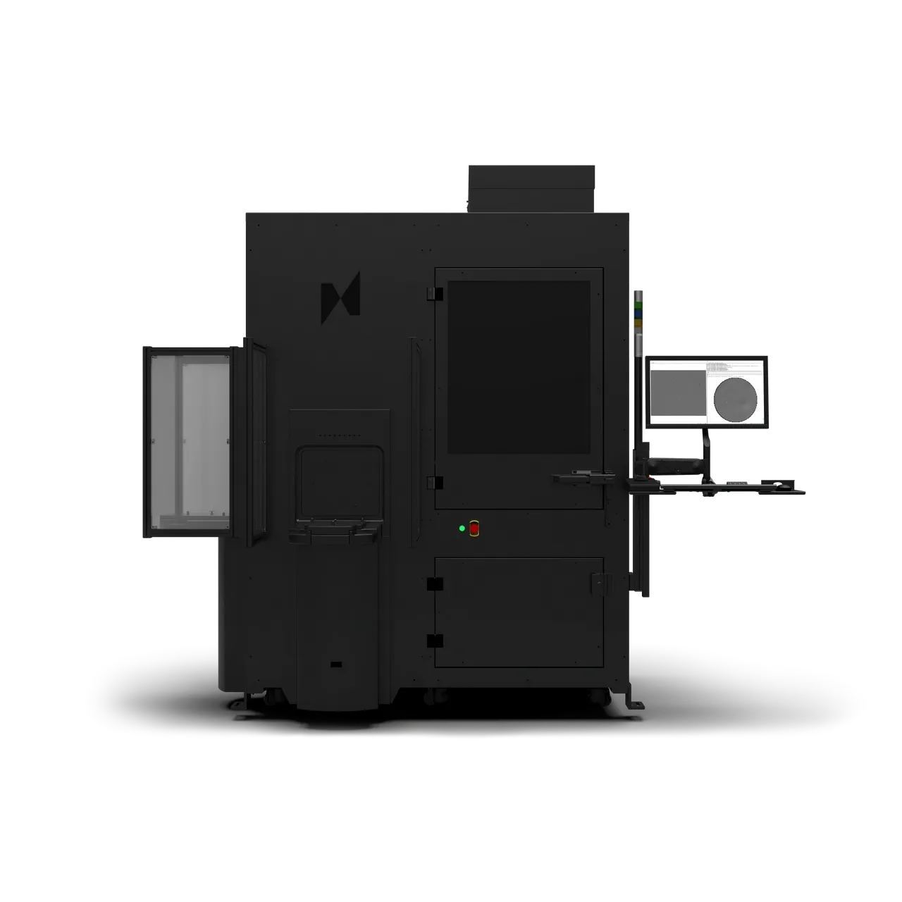
nSpec CPS
An ideal system for high‑volume manufacturing environments with robotic handling capabilities.
Need help selecting a configuration? We can recommend optics, automation level, and workflow based on your wafer/material and defect types.
SWS‑tec — Non‑contact eddy‑current measurement
SWS‑tec provides non-contact measurement solutions using eddy‑current based technology for sheet resistance, resistivity and thin‑film thickness — designed to protect delicate samples while delivering repeatable results.
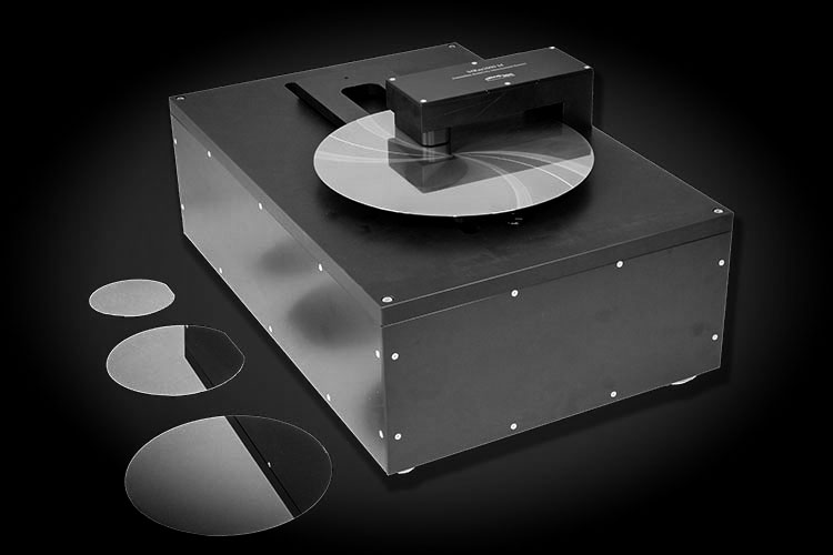
MRes 2000 — Contactless resistivity measurement
A non-contact resistivity measurement system designed for industry and research, accommodating wafer diameters up to 300 mm. Suitable for bulk and conductive layer measurements, with automated mapping options.
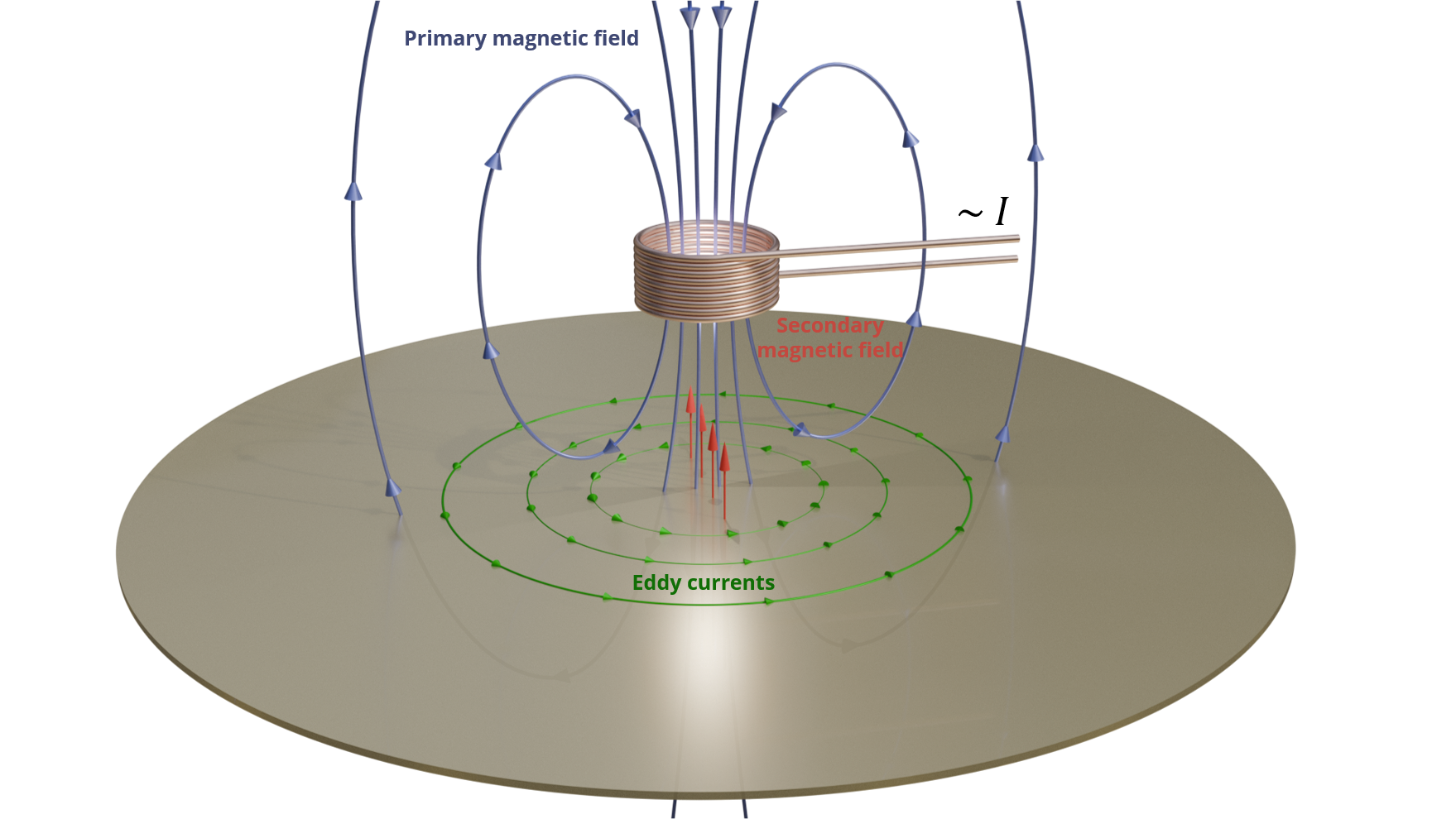
Eddy-current measurement — why it matters
Non-contact measurement avoids probe marks and sample alteration. Eddy currents induced by a coil interact with the sample; analyzing the response enables sheet resistance / resistivity and thickness characterization in a non-destructive way.
We support integration into lab and production environments and can advise on measurement recipes and calibration practices.